"विद्यार्थी लभते विद्याम्"
"One who aspires wisdom, attains it."
News
Latest developments & highlights
DEC 15
IIT Patna secures 9th Rank in the 58th Inter IIT Sports Meet that t...
IIT Patna achieved an impressive 9th rank in the 58th Inter IIT Sports Meet held at IIT Hyderabad, showcasing the athletic prowess and competitive spirit of its students.
MAR 27
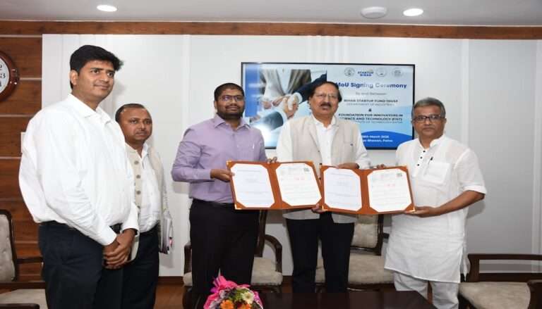
Memorandum of Understanding (MoU) signed between the Department of ...
A Memorandum of Understanding (MoU) has been signed between the Department of Industries, Government of Bihar, and the Indian Institute of Technology (IIT) Patna for the establishment of a Rapid Prototyping Lab, aimed at fostering innovation and accelerating product development in the region.
AUG 2
Publication of Blog on the United Nations: UNESCAP Website
The blog on the United Nations and UNESCAP website has been published.
JUN 27
1st rank among emerging government colleges established in/after 2000
IIT Patna has secured the first rank among emerging government colleges established in/after 2000.
JAN 30
Dr. Amarnath Hegde has been selected for 'Reviewer of the year 2019...
Dr. Amarnath Hegde has been selected for 'Reviewer of the year 2019' award in non-editorial board member (non-EBM) category by Indian Geotechnical Society.
Notices
Important updates & announcements
MAY 23
IIT Patna hosts inter iit tech meet 14.0
IIT Patna successfully hosted the Inter IIT Tech Meet 14.0, bringing together the brightest minds from across the Indian Institutes of Technology to compete in innovative technology challenges and foster collaboration.
MAY 21
Advt. R&D/1231/SCM/473
IIT Patna is inviting applications for the post of Junior Research Fellow (JRF) in the Department of Computer Science and Engineering.
MAY 20
Advt.R&D/1020/LCG/472 DATED: 20.05.2025 for the po
IIT Patna is inviting applications for the post of Technical Assistant in the Department of Computer Science and Engineering.
MAY 16
Advt. R&D/1267/DOI/471
IIT Patna is inviting applications for the post of Research Engineer, Junior Research Fellow (JRF) and Research Intern in the Department of Computer Science and Engineering.
Career
Join our team of innovators
MAR 18
Junior Research Fellow (JRF) - 02 posts
Verification and Validation of geotechnical design and behavior predication...
Research Impact
Innovation driven by discovery.
88+
Patents Filed
₹500+Cr
Research Funding
400+
Publications
17+
Startups
Centers of Excellence
Interdisciplinary hubs tackling global challenges.
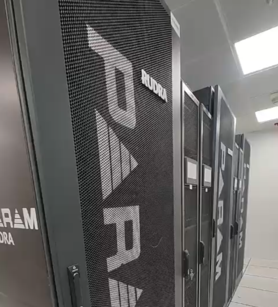
Aryabhatta Supercomputing Centre
ASC, under the National Supercomputing Mission, powers IIT Patna’s HPC with PARAM Rudra.
PHN Technology Centre
Pioneering research in Robotics, AI and IoT aimed at bridging the gap between academia and industry via cutting-edge technologies.
Academics
Interdisciplinary hubs tackling global challenges.
Bachelors
A rigorous undergraduate program focused on strong fundamentals, innovation, and industry ready skills.
Masters
Advanced coursework and research opportunities designed to deepen scientific knowledge and analytical thinking.
Doctorate
A research intensive doctoral pathway enabling scholars to contribute to cutting-edge knowledge and innovation.

